
Stamped Conductive Parts
Custom copper and copper-alloy contact blades, terminals, conductive bars and supports, stamped and formed to your drawing for relay, switch and contactor assemblies.
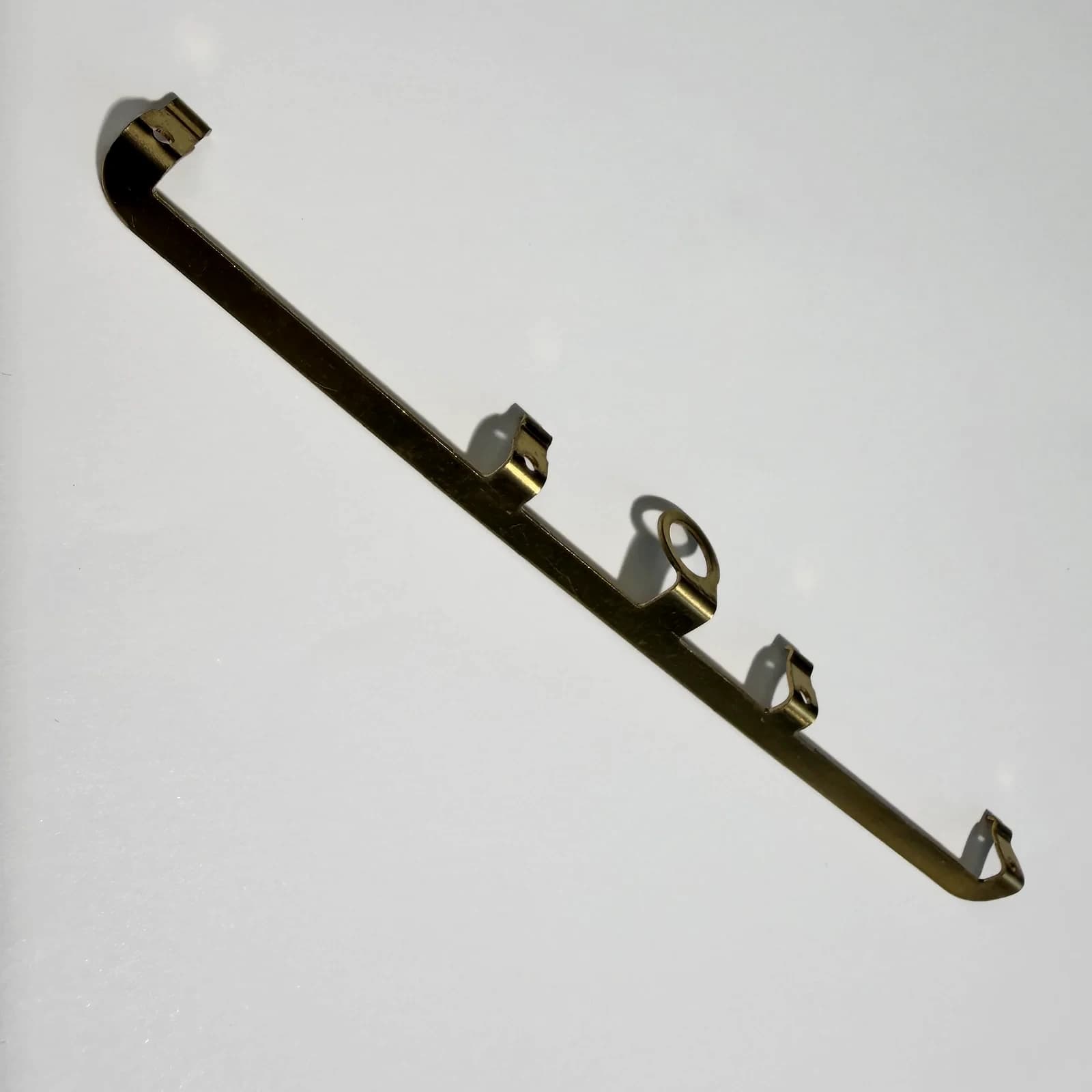
- Materials
- Cu, copper alloys, steel, iron, silver, and specified materials
- Applications
- Relays, switches, contactors, circuit breakers
- Reference size
- Key profile and feature dimensions confirmed by drawing or sample
- Part geometry
- Confirmed from the drawing or sample
- Material and temper
- Confirmed from the drawing or sample
- Base material and surface condition
- Confirmed from the drawing or sample
- Inspection requirements
- Confirmed from the drawing or sample
Definition
Custom copper and copper-alloy contact blades, terminals, conductive bars and supports, stamped and formed to your drawing for relay, switch and contactor assemblies.
Development
Requirement clarification, drawing or sample checks, preliminary feasibility, sample development, and process verification support a final production quotation.
- Contact blades and supports: Stamped conductive carriers can be supplied as individual parts or as part of a riveted or welded contact assembly.
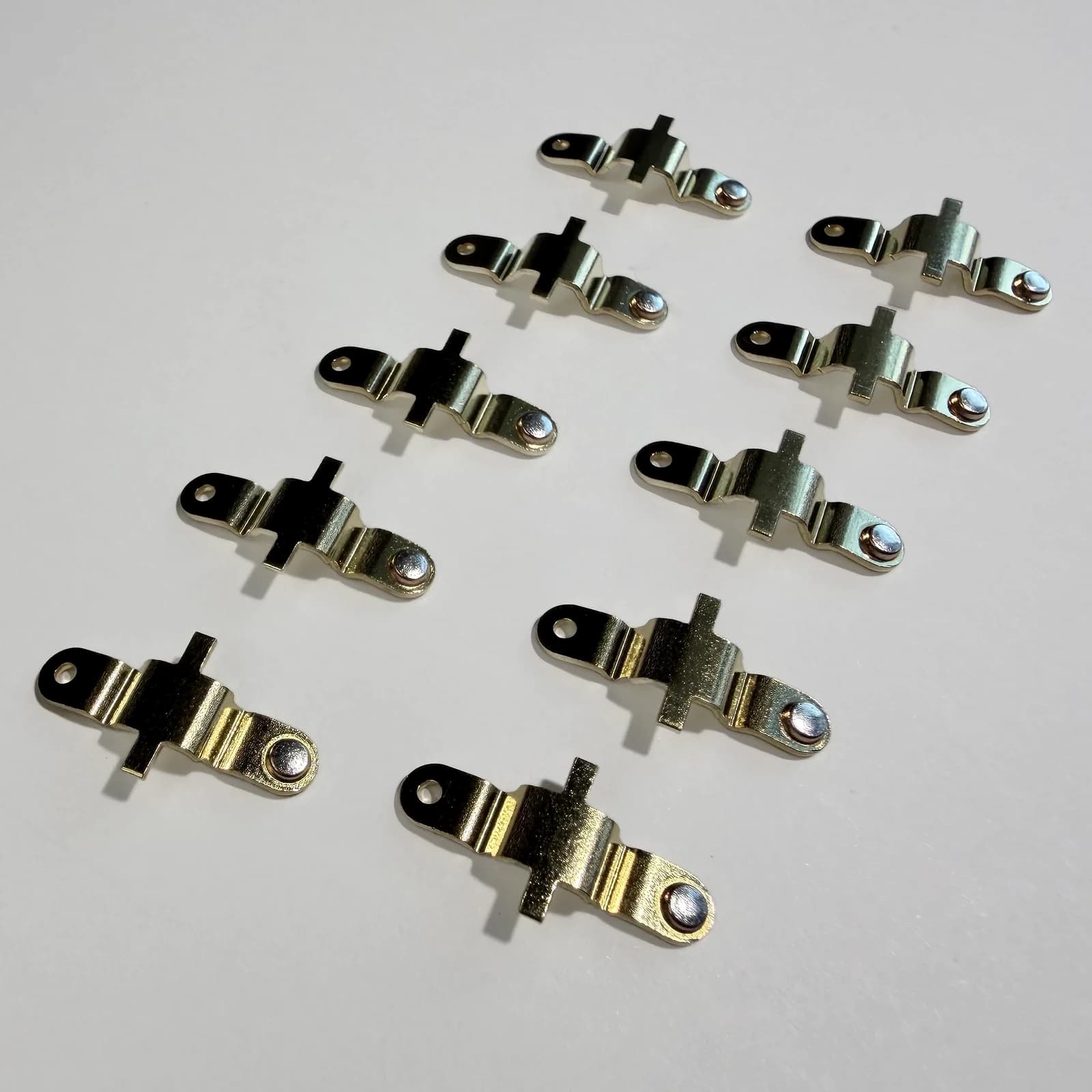
- Terminals and conductive links: Develop the profile, holes, bends and connection features for your electrical assembly, using the specified material and temper.
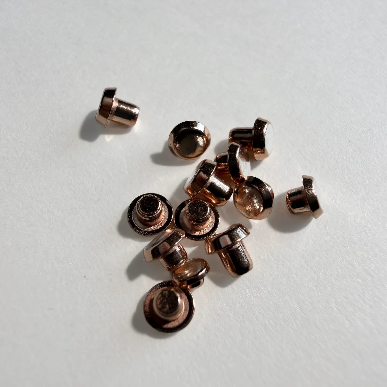
- Base material and finish: Confirm the base material and required surface condition, such as bare copper, silver plating, or a specified silver contact feature.
- Sampling and repeat supply: Production generally starts at 100 pieces per part number per order. Tooling, sample cost and the production specification are confirmed for the particular part.
Stamped-part dimensions
Confirm the base material, thickness, blank profile, holes, bends, and surface condition before tooling.
- Base material, thickness, and temper where specified
- Blank profile, hole pattern, bend features, and formed geometry
- Key dimensions, hole spacing, bend angles, and specified tolerances
- Surface condition and any riveted or welded assembly relationship
| Dimension | How confirmed |
|---|---|
| Base material and temper | Drawing or sample |
| Section thickness | Drawing or sample |
| Blank profile / flat dimensions | Drawing or sample |
| Hole diameter and spacing | Drawing or sample |
| Bend features, angles, and radii | Drawing or sample |
| Critical dimensions and tolerances | Technical review |
Confirm these dimensions and tolerances from the drawing or sample, material system, and project review before production.
Manufacturing & Inspection
Manufacturing
The required features and assembly interface determine the stamping and forming route.
- Punching and blanking
- Bending and drawing where required
- Coining, embossing, or tapping where required
- Integrated riveting or welding where the part is supplied as an assembly
Inspection
Checks focus on the functional features that make the stamped part repeatable in the target assembly.
- Blank profile, holes, bends, and critical dimensions
- Visual condition and surface condition
- Dimensional consistency for specified features
- Strength or assembly-related checks where specified
Additional stamped-part forms.
These examples show additional stamped conductive forms. Final geometry and features are confirmed from your drawing or sample.
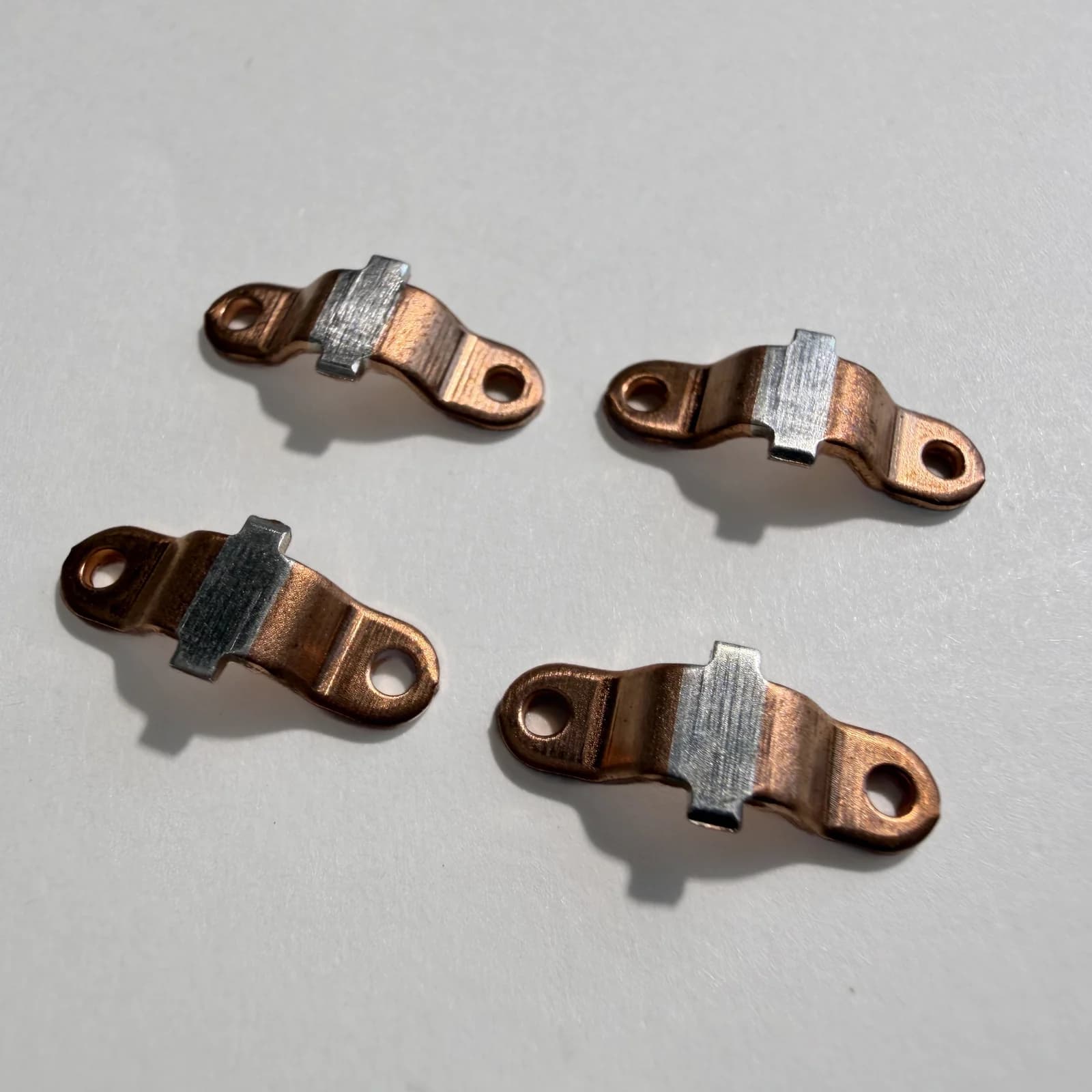
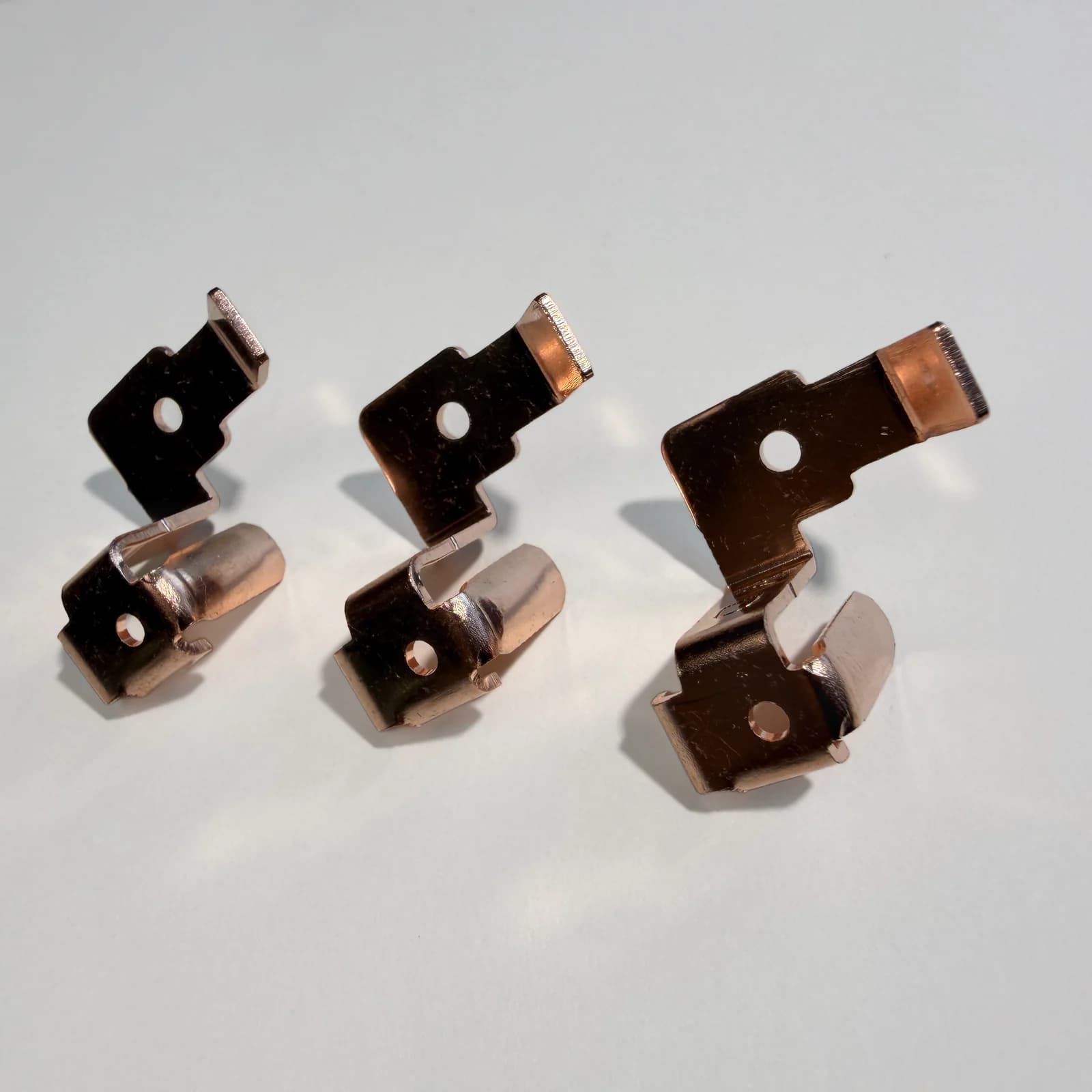
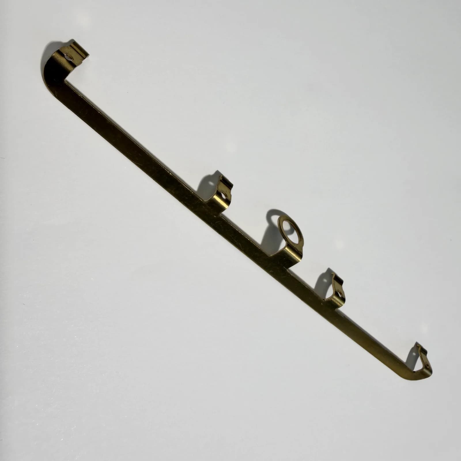
Examples show available forms and production scenes. Final materials, dimensions, surface condition, and process are confirmed from the drawing, sample, and project review.
Related products
Products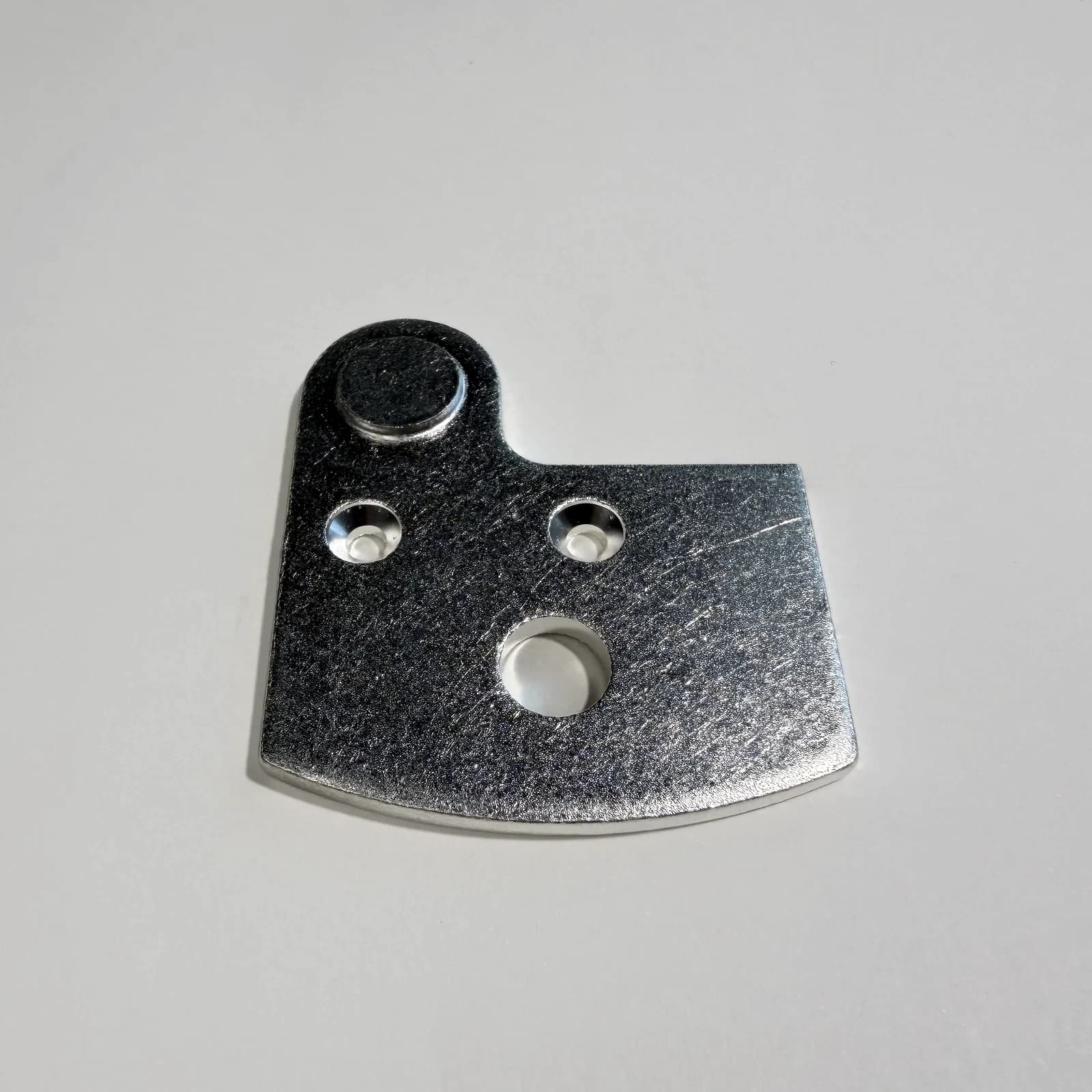
Sample and quote
Share the base material, thickness, bends, holes, surface condition, drawing, or sample before production. Include the drawing or sample reference, expected quantity, and required timing. Typical MOQ: 100 pcs per part number per order. Sample lead time: typically 5-10 working days after technical review and agreed start conditions. Production lead time: typically 15-25 working days after technical review and agreed start conditions.